


Strain Rate Measurements on Printed Circuit Boards (PCBs)

April 17, 2023
The strain analysis of printed circuit boards represents complex but crucial work, as these components are used in mission-critical applications. Next to Finite Element Analysis (FEA), the testing process involves strain gauge installation, measurements, and data interpretation, based on which engineers can make decisions and define the next steps.
Introduction
Designing instrumentation for harsh environments requires knowledge of and in-depth testing for durability and thermal or mechanical impacts.
In this paper, I will discuss how to perform strain rate measurements on Printed Circuit Boards (PCBs) whether single-sided, double-sided, or multi-layered. By reading this you will:
Understand why strain measurements are performed on PCB designs,
Requirements and standardization of PCB testing,
How to select and measure strain on PCBs,
How to install the strain gauges on the PCB,
Data acquisition instruments and setup of DewesoftX software,
Data analysis and reporting in DewesoftX.
What are PCBs?
A PCB (Printed Circuit Board) is a board made of insulating material - such as fiberglass or plastic - on which conductive pathways and electronic components are mounted. It is used to mechanically support and electrically connect electronic components using conductive pathways, or traces, etched from copper sheets laminated onto the non-conductive substrate.
PCBs are widely used in the electronics industry to connect and control electronic components such as resistors, capacitors, and integrated circuits. The PCB design can vary greatly depending on the type of application and the complexity of the circuitry required. Single-layer, double-layer, and multi-layer PCBs are common, with the latter offering greater complexity and flexibility in circuit design.
The process of designing and manufacturing PCBs involves specialized software and equipment, including computer-aided design (CAD) software, etching machines, and automated assembly equipment. PCBs have become an essential component in the electronics industry due to their reliability, low cost, and ability to support high-density circuitry.
Why strain measurements on PCBs
As we evolve and humanity ever advances, the amount of electronics (consumer and professional electronics) in our daily lives is dramatically increasing. New technologies, such as autonomous vehicles, smartphones, and other smart devices, exponentially increase our dependency on reliable electronic components.
At the same time, the requirements for electronics are changing. They must be more powerful and compact, lighter, durable, and, of course, at a minimum price! To harmonize and still have high-performance and reliable electronics with a solid price requires extensive testing of the complete instrument and every component. And this will naturally include the PCBs.


So, where in the manufacturing process are the most common malfunctions and stresses happening?
During the positioning of the components on the PCB in the pick-and-place machine,
Bending of the PCB during installation of connectors, heat sinks, or other bigger components,
Broken SMD capacitors due to high bending stress in other steps of the production process,
Tightening screws or fitting the PCB into the chassis,
Mechanical or vibration impacts during the transport,
Thermal effect (in the production process, testing, or end-user usage) resulting in cracks due to thermal expansions.
And many other impacts could happen in the process and must be characterized individually by electronics manufacturers.
All of the above points can lead to short and long-term component failures. Potentially, these could lead to catastrophic results.
Requirements and standardization of PCB testing
The importance of electronic components in mission-critical applications has established an extensive guide and methodology on how, what, and where. The most important documentation for such guidance is IPC-JEDEC 9701-9706. It’s required for almost every space application.
In addition to these documents, internal documents/requirements are also made based on the expected usage of the electronics. These documents cover not only strain rate measurements but also thermal, vibration, and shock measurements performed on the PCB.


How to measure and where to mount the strain gauge
Unfortunately, for numerical and simulation methods such as FEA, there are limitations as it traditionally is based on perfect mathematical modeling. PCB structures often utilize fibrous materials where the granular direction is extremely difficult to model. In the case of PCBs, which are heterogeneous in their material properties, this is not simple to do with very high accuracy. It is also almost impossible to cover the complete production cycle.
Therefore, physical tests on real PCBs must be performed, not just to confirm loading patterns, plains, and cycles but to confirm the validity of existing model load cases. A real measurement with strain gauges is the only reliable and accurate measurement that provides the real strain behavior of the board. Other test methods, such as CT and X-ray, do not provide good enough results and are usually static.
Selection of strain gauge
In general, for such a PCB strain measurement strain gauges could be the uni-axial - linear pattern - or rosette strain gauges. Uni-axial linear pattern strain gauges are used to measure strain in a single direction, while rosettes make three independent measurements in different directions. This depends a lot on expectations or knowledge in which direction the deformation of the PCB will happen. In most cases, engineers mount rosettes, as they reveal the “Unknown” deformations, directional information, and principal stresses and strains.
The strain gauge itself should be very small with a sensor size as small as 1 to 2 mm2. As standard both 120 and 350 Ω resistors could be used. However, due to grid self-heating issues having a higher resistance on the smaller gauge allows a little bit higher excitation without having stability problems. PCBs are not very good heat sinks.
Typically, with such a small sensor the excitation voltage will be 2 V or less but still high enough to have a good signal-to-noise ratio. Keep in mind that if energized the very PCB and its components could be a source of noise!


An important factor to consider when choosing a strain gauge is also environmental temperature - where it is planned to be used. In the case of performing thermal cycling or measurements of the PCB while traveling through the oven, a higher temperature range strain gauge should be used.
Where to measure
As all these tests consume time and money, it’s not feasible to place strain gauges in every location. Suppliers and users therefore normally agree on which components such a strain measurement should be performed. But if this is not the case below are a few recommendations coming from IPC-JEDEC-9704A.
Area Array Components
Any area array device with a package body size equal to or larger than 27 x 27 mm or finer pitch components - 0.8 mm pitch and below - with a body size > 10 mm should be evaluated. If there are several fine pitch components, the worst-case locations - minimum three - based on engineering judgment, history of damage, or Finite Element Analysis should be tested.
Non-Area Array Components
The interconnects in non-area array components with smaller solder joints and stiff bodies - i.e., Multilayer Ceramic Capacitor (MLCC) - are also susceptible to strain-induced solder joint failures. By evaluating the strain generated during these processes, and ensuring they remain within acceptable limits, failures can be significantly minimized or eliminated. Failures such as solder joint cracking, device fracture, pad lifting, pad cratering, and printed wiring board conductor damage.


How to install a strain gauge on the PCB
One of the most important parts of the measurements is the proper installation of the strain gauge and PCB preparation. This will ensure the proper connection between the wiring board and the strain gauge and thus provide accurate and reliable results. In general, manufacturers provide instructions on how to properly install the strain gauge on the PCB. However, below are a few recommendations for installation:
Degreasing the surface of where the strain gauge will be attached with a solvent such as Isopropyl alcohol, using caution as some chemicals can affect the surface itself!
Light abrasion of the surface so that the adhesive can stick better onto the PCB and provide proper bonding with the strain gauge. For this step, Silicon Carbide Paper or Abrasive Paper (400+) should be used to lightly scuff the surface. The conformal coating should be removed when applying strain gauges as it can influence the bonding between PCB and the sensor. It can generate inaccuracies during the measurement if it impacts the PCB structure or other processes. It should be applied on top of the strain gauge after protecting the gauge grid area.
Clean the surface again with a solvent such as Isopropyl alcohol.
Most adhesives require a certain pH value on the surface to function and glue properly on the board. A neutralizer should be applied on the surface.
Before gluing the strain gauge, it is essential to decide and align the direction of all of the strain gauges - this will make life easier in the measurement/analysis portion.


Attach the strain gauge and wires on the surface according to the manufacturer’s instructions with gauge installation tape and proper adhesive. Then, it is time to connect the strain gauge to the measurement amplifier.
Use a 3- or 4-wire configuration. A 2-wire can introduce a significant thermal error due to cable length.
The cable length between the strain gauges and measurement amplifier has no physical limitations due to lead wire compensation. However, as a rule of thumb, the resistance of the cable should be < 10% of that of the strain gauge. In case of electrical noise, use a twisted shielded cable.
Data acquisition and software setup
Data acquisition instruments
The specifications of the instrumentation/strain amplifier are crucial factors in PCB strain measurement:
The sampling on DAQ should be simultaneous, as multiplexed or sequential sampling may result in miscalculated strain values due to phase differences between channels.
For In-Circuit Tests (ICT) and Board Functional Tests (BFT), a sampling rate of > 500 Hz is recommended, and 1-2 kHz is normally used. Depending on test procedures, the sampling could even go beyond 50 kHz, for example, when it includes shock/drop testing.
The minimum sampling resolution should be 16 bits.
It is recommended to have built-in 3-wire quarter bridge support - not providing this externally - and bridge imbalance compensation. Ultimately, this reduces the time spent as well as potential additional variables.
It is good to have a built-in low pass filter to remove noise during strain gauge collection.
The amplifier should be capable of providing an excitation of at least 2V. Due to heating, it is the most general voltage in such applications with small sensors. The possibility of even lower excitations in case heating could be problematic.
What is nice to have in addition:
Synchronized measurement of temperature sensors for additional thermal tests or measurements inside the oven.
Ability to connect other types of sensors, like accelerometers and pressure signals. These could, for instance, intercept the load fixture data or other phenomena of processes where the strain rate is just one facet of the test.
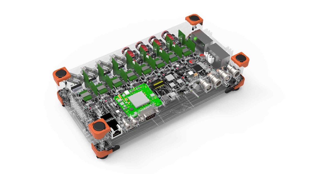
Such a universal measurement device is the SIRIUS data acquisition instrument from Dewesoft. It fulfills all the above requirements, including thermal and high-speed acceleration measurements. And is still a compact and robust tool for such measurements:


Simultaneous sample rate of up to 200 kHz per channel for even the most extreme high-speed drop tests,
Accuracy down to 0.05 %,
24-bit resolution with built-in bridge completion for half and 3-wire quarter 120/350Ω bridge measurements,
Lead wire compensation,
Shunt and short functionality to check drift of sensor and amplifier before performing a measurement,
Programmable excitation from 0 up to 12V
Built-in low pass filtering, to remove noise on the strain gauges.
Other important information while performing the measurement:
While the PCB is at rest, the strain value shouldn’t drift. If it does, lower the excitation value should until this effect disappears.
As the measurement of strain gauges generally requires high accuracy, the applied instrumentation should be calibrated according to the manufacturer’s recommendations.
Repeat each step at least three times to capture the natural variation of the subject assembly step.
Software configuration and measurements
Every test engineer needs to receive measurement results as quickly and smoothly as possible. The DewesoftX software is outstandingly easy to use and quick to configure. The software is included with the SIRIUS devices and has free lifetime updates - it is a guaranteed solution for the future.
Measuring on five Circular rosettes involves the configuration of 15 input channels:
Quarter 3-wire 350 Ω bridge measurement type,
Low pass filter to remove the noise,
Excitation 2V (depending on the surface),
Compensation for lead wires with an integrated automatic check.


Neat software/hardware function enables/disables the Shunt resistor and shortens the amplifier. This becomes even more useful for measuring a longer process and during thermal cycling. Simply shunting/shorting at the beginning and end of the measurement, it will tell if any drift off the amplifier or sensors occurred.
A quick overview of the measured data:


Data analysis and reporting in DewesoftX
Once the data recording is done, the evaluation and report are generated. A Math module built inside the Dewesoft Math Library is made for PCB Strain Rate calculations either according to the IPC/JEDEC-9704 standard or a custom company threshold. To perform the calculations, the module is enabled, and details of the limitations and PCB are inserted. This calculation can be done online - during the measurement - and offline after the measurement is finished.


Select the measured strain gauge channels on the left side (Epsilon A, B, C),
Pick the Threshold type, based on which the calculations are done,
From PCB thickness – threshold values according to the IPC/JEDEC-9704 standard,
From threshold value – used for custom threshold values (for instance internal company standards),
PCB thickness – thickness of PCB in mm,
Threshold value - used for custom calculations with Threshold type from the Threshold value,
Minimum strain rate on the reference curve (used only for visualization of the data),
Maximum strain rate on the reference curve (used only for visualization of the data),
Output epsilon A, B, C, D channels – additional calculation of Epsilon 4.
Calculations and threshold definitions by IPC/JEDEC-9704 standard
The calculations performed are explained below:
Maximum Principal Strain :
Minimum Principal Strain :
Diagonal strain :
Strain rates:
: Strain, : Time
In case the threshold from IPC/JEDEC-9704 standard is used, it is calculated as:
Such a graph, where Strain Rate against Principal/Maximum strain are shown in Figure 10, where guideline limitations from IPC/JEDEC-9704A are shown.
Typical report


Correct data interpretation is essential, and it is up to the measurement engineer to ensure the relevant values are reported. Using a combination of overall minimum, maximum, absolute, and diagonal strain is the key to the engineer making the right decisions. The PCB strain rate math tool provided by Dewesoft can automatically report PASS/FAIL conditions, based on the defined threshold limits.

